An international team of researchers has developed a method of imaging what occurs at the boundary between 2D and 3D materials, revealing ways to control the electronic properties of atomically thin materials.
Atomically thin materials can be modified by stacking two layers together and rotating one slightly in relation to the other. This creates what are known as moiré patterns, where tiny shifts in the alignment of atoms between the two sheets create larger-scale patterns. 2D materials must at some point connect with 3D materials. An international team has now developed a method of imaging what occurs at these interfaces, down to the level of individual atoms, and of correlating the moiré patterns at the boundary between 2D and 3D materials with the resulting changes in the material’s properties.
The new findings are described in the journal Nature Communications, in a paper by MIT graduate students Kate Reidy and Georgios Varnavides, professors of materials science and engineering Frances Ross, Jim LeBeau, and Polina Anikeeva, and five others at MIT, Harvard University, and the University of Victoria in Canada.
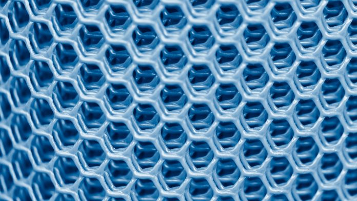
Pairs of 2D materials such as graphene or hexagonal boron nitride can exhibit a wide range of variations in their behaviour when the two sheets are just slightly twisted relative to each other. That causes the chicken-wire-like atomic lattices to form moiré patterns. In the case of 2D materials, Ross explained: “It seems like anything, every interesting materials property you can think of, you can somehow modulate or change by twisting the 2D materials with respect to each other.”
Imaging the 2D-3D boundary
The team used two unique transmission electron microscopes that enable a combination of capabilities that is unrivalled in the world. In one of these instruments, a microscope is connected directly to a fabrication system so that samples can be produced onsite by deposition processes and immediately fed straight into the imaging system. This is one of only a few such facilities worldwide, which use an ultrahigh vacuum system that prevents even the tiniest of impurities from contaminating the sample as the 2D-3D interface is being prepared. The second instrument is a scanning transmission electron microscope. This microscope has outstanding stability for high-resolution imaging, as well as multiple imaging modes for collecting information about the sample.
The team needed to figure out how to reveal the atomic configurations and orientations of the different layers. A scanning transmission electron microscope produces more information than is apparent in a flat image. This data can be separated out so that the information at all points in an image can be used to decode the actual solid structure.
The researchers used a combination of techniques called 4D STEM and integrated differential phase contrast to achieve that process of extracting the full structure at the interface from the image. The researchers showed through modelling that electronic properties are expected to be modified in a way that can only be understood if the full structure of the interface is included in the physical theory.
Ross says the findings could help lead to improved kinds of junctions in some microchips, for example. She explained: “Every 2D material that’s used in a device has to exist in the 3D world, and so it has to have a junction somehow with three-dimensional materials,” she says. So, with this better understanding of those interfaces, and new ways to study them in action, “we’re in good shape for making structures with desirable properties in a kind of planned rather than ad hoc way.”


