Dr Līga Grīnberga from the Institute of Solid State Physics, University of Latvia introduces the revolutionary CAMART2 project, helping to take innovative technology out of the laboratory and into the real world.
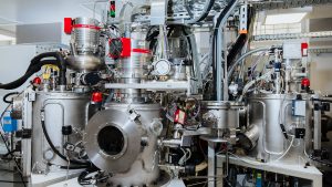
The Institute of Solid State Physics, University of Latvia (ISSP UL) is one of the leading research institutions in Latvia – the strong foundations of which were laid 45 years ago. It is also the place where, since 2017, the CAMART2 project (Excellence Centre of Advanced Materials Research and Technology Transfer) has raised research capabilities by implementing new research strategies and developing infrastructure to fortify the institute’s priority research directions – which include materials science, nanotechnology, thin films, photonics, and micro and nanoelectronics. The project has also utilised a new approach to direct fundamental research toward technological needs and industrial challenges. The set-up established within the framework of the CAMART2 has contributed to the development of advanced, unique, and commercialisable technologies.

TESS
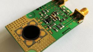
It is not unusual that, while researching one thing, something unexpected comes out of it. One of the innovations created at the ISSP UL is the thermoelectric sensor, which came into existence while developing a thin film organic thermoelectric generator. This innovative technology – the high-speed thermoelectric electromagnetic radiation sensor (TESS) – won one of the Latvian Academy of Sciences’ Most Important Achievements in Applied Science awards in 2021.
The new sensor device is especially useful in controlling power in various laser technologies. The innovative technology created by the scientists of the ISSP UL’s Laboratory of Organic Materials is 1,000 times faster than sensors existing today on the market of thermoelectric sensors. Up to now, thermoelectric sensors were capable of measuring laser power averaged in time, typically averaging many individual impulses. The new thermoelectric sensor can characterise each laser impulse individually. The capacity of this device to measure and control every impulse is particularly important everywhere a laser is used to modify the characteristics of materials. This includes laser welding, cutting, engraving, and numerous laser surgery applications.
The innovative technology allows for the measurement of high-speed laser power in wide spectral diapason from ultraviolet to far infrared light. The technology itself is based on the thermoelectric effect in thin films. The exceptionality of the device’s properties lies in the unique properties of the organic material used by the scientists. The material’s very low thermal conductivity is combined with the comparatively high material’s ability to convert the heat gradient into electricity (characterised by the Seebeck coefficient). These combinations of properties provided an opportunity to create a sensor based on thin films that can generate a signal strong enough to be read out from a single laser pulse. At the same time, the employment of films with submicron thickness allows for the creation of a sensor with exceptionally low heat capacity; therefore, the device can operate at a very high speed and in an infrared spectrum region where classic semiconductors do not work. This allows for characterising individual laser impulses, which until now was practically impossible.

Using such sensors in various tools based on laser technology will allow them to be operated more effectively and faster and might also develop new possibilities. In laser surgery, the new sensor will allow for performing various surgeries more quickly and accurately. For example, endovenous ablation surgery can be done much quicker by being able to control the power of each laser impulse and therefore administer the necessary dose in a shorter time and more precisely.
One of the creators of TESS, Dr Mārtiņš Rutkis, said: “TESS once again confirmed my conviction that, if someone is investigating a phenomenon or developing a specific product, they should be open-minded and ready for a completely unexpected opportunity to appear. And, when it happens, the researcher must be brave enough to take this new pathway to success.”
The thermoelectric sensor is patented in the European Union, the USA, Japan, and China. A licensing and technology transfer contract was signed with Thorlabs, a leading designer and manufacturer of photonics equipment for research, manufacturing, and biomedical applications.
Organ-on-a-chip technology
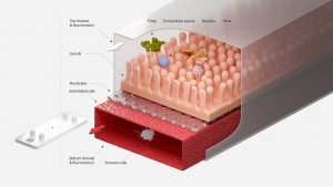
From the very beginning, the aim of the joint work of the researchers from the ISSP UL’s Micro and Nanodevices Laboratory and Latvian Biomedical Research Center was to create a unique organ-on-a-chip device – a miniature artificial organ or replica of an organ outside the human body. It is a polymer device with microchannels inside. It is called a chip because it is mostly made using semiconductor technology, the same technology that makes almost every modern electronic device possible. The organ-on-a-chip does not replace real organs but serves as a test model.
Followed by a lung-on-a-chip, the first device created by scientists is a gut-on-a-chip. It allows for testing the effect of drugs, obtaining more information than from in vitro models used so far. Researchers explain that the gut contains villi structures that cannot be replicated by growing cells in a petri dish. Of course, there is the alternative to test the drugs on animals, which have the desired cellular activity and structure, but animal intestine, with its microbiota, is significantly different from that of a human.

There are several fields this innovative technology could be applied in: pharmaceutical (drug and vaccine testing), production of food additives and pesticides (safety testing), and the space industry (determining the right combination of probiotics for astronauts). The technology means that diseases, such as cancer and various digestive system diseases, could be grown on chips. This way, it will be possible to see how a drug affects an individual, should they have specific conditions. Eventually, this innovative technology could also be used in personalised or precision medicine. Scientists behind the technology suggest that, in the future, everyone will be able to have their organs on chips created from their stem cells, which could be stored in a special bank. When the need for more serious treatment arises, the doctor can check the chip and find the most appropriate drugs, rather than giving different medications on a trial basis until there is a significant improvement in the patient’s health.
The scientists who have developed organ-on-a-chip technology in Latvia have founded a biotechnology start-up called Cellbox Labs, which bought the intellectual property associated with the invention from the Institute of Solid State Physics.
Dr Gatis Mozoļevskis, Leader of the Micro and Nanodevices Laboratory and Co-founder and CEO of Cellbox Labs, said: “We are optimistic about the fact that, by attracting investments, in time we can be another of Latvia’s unicorn companies. This idea and field have an immense potential to revolutionise drug discovery and patient treatment processes, thereby paving the way towards more accessible healthcare to everyone. Right now, we are well positioned to deliver the yet unlocked potential of the technology!”
These research, development, and commercialisation activities are supported by the ISSP UL’s Horizon 2020 Teaming project CAMART2, which is one of the most significant projects in Latvian science, and received European Commission funding for strategic development with the assistance of the top players in the field from Sweden – Royal Institute of Technology (KTH) and Research Institutes of Sweden (RISE). The project’s objective is to strengthen the ISSP UL’s position as a significant regional science, innovation, and technology transfer centre and to strengthen the Latvian state’s position in Europe and internationally.

Dr Līga Grīnberga
CAMART² WP5 leader
Institute of Solid State Physics
University of Latvia
http://www.cfi.lu.lv/en
Liga.Grinberga@cfi.lu.lv
Please note, this article will also appear in the twelfth edition of our quarterly publication.


