The European Commission has approved a €1.3bn funding initiative to support the establishment of a semiconductor advanced packaging and testing facility in Novara, Italy.
The initiative, led by Silicon Box, is part of a broader strategy to strengthen Europe’s semiconductor production industry.
This move aligns with the European Chips Act and the European Commission’s 2024-2029 Political Guidelines, aiming to enhance the EU’s security of supply and technological autonomy in a critical sector.
The development follows the recent major news of €5bn EU funding to support a semiconductor manufacturing plant in Dresden, Germany.
Teresa Ribera, Executive Vice-President for Clean, Just and Competitive Transition, commented: “The €1.3bn Italian measure approved today supports a first-of-a-kind facility for advanced packaging of chips.
“It ensures that key players in the telecommunications, automotive, or consumer electronics sectors have access to high-performant, reliable and energy-efficient chips.
“This will support our digital and green transitions and help create high-skilled employment. At the same time, we ensure that possible distortions of competition are limited.”
Boosting Europe’s semiconductor independence
Semiconductors are integral to modern technology, powering devices and systems ranging from smartphones to advanced vehicles.
Recent global supply chain disruptions have underscored the urgent need for Europe to increase its production capacity and reduce reliance on external suppliers.
The European Chips Act, introduced in February 2022 and enacted in September 2023, is a comprehensive legislative framework designed to address these challenges.
It promotes investments in semiconductor infrastructure, safeguards the EU’s supply chain resilience, and supports technological innovation.
The approval of Silicon Box’s semiconductor advanced packaging project marks the fifth major decision under the Chips Act, demonstrating the EU’s dedication to reinforcing its semiconductor ecosystem.
This new facility is expected to play a pivotal role in advancing Europe’s capabilities in semiconductor packaging and testing technologies.
Inside Italy’s semiconductor packaging project
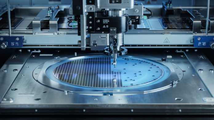
The €1.3bn in direct funding will supplement Silicon Box’s €3.2bn investment in the new facility. This advanced plant will focus on semiconductor advanced packaging, a process that integrates multiple chips, known as ‘chiplets,’ into a single package.
This innovation enhances the chips’ performance and energy efficiency, making them more effective for a range of applications.
Unlike traditional wafer-level packaging methods, the Novara facility will employ panel-level packaging combined with innovative 3D integration techniques.
This approach will enable the production of highly efficient multi-chip modules. Once fully operational, the facility is expected to process approximately 10,000 panels per week, with full capacity anticipated by 2033.
The plant will carry out critical stages of semiconductor production, including chip assembly, advanced packaging, and comprehensive testing.
These capabilities are expected to significantly enhance Europe’s semiconductor manufacturing capacity while fostering innovation in the development of next-generation technologies
Benefits and long-term commitments
The Silicon Box project is expected to deliver far-reaching benefits to the EU’s semiconductor ecosystem.
The new facility will strengthen Europe’s semiconductor value chain by providing advanced packaging solutions that create opportunities for collaboration and growth across the industry.
Silicon Box has also committed to advancing the development of cutting-edge packaging technologies, positioning the EU as a global leader in this field.
Furthermore, the project is designed to address supply chain vulnerabilities by prioritising critical orders during times of shortage, as mandated by the European Chips Act.
In addition to these industrial benefits, the initiative will contribute to workforce development. Silicon Box will establish comprehensive training and educational programmes to build a pool of highly skilled professionals. This effort will ensure a sustainable pipeline of talent to support Europe’s expanding semiconductor industry.
A landmark move toward semiconductor sovereignty
By supporting the establishment of a state-of-the-art semiconductor advanced packaging facility, the EU is reducing its dependency on external suppliers while fostering innovation and economic growth.
The Novara facility is poised to become a cornerstone of Europe’s semiconductor strategy, driving the development of advanced technologies and ensuring supply chain resilience.
As the EU continues to strengthen its position in this vital sector, it is laying the groundwork for long-term competitiveness and technological leadership in a rapidly evolving global landscape.


