Wrocław University of Science and Technology, Poland, outlines its goals, activities and international collaboration in the modern fields of nanoscience and nanotechnology
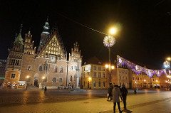
Wrocław University of Science and Technology (WUST) is a leading technical university of Poland. The city, the regional capital of Lower Silesia, is also one of Poland’s major academic and economic centres, hosting several public and private universities.
WUST is the city’s largest university with 33,000 students and 2,000 academic staff and, in recent years, has undergone rapid development and significant growth through unprecedented investment in new laboratories and modern infrastructure.
By restructuring old faculties and departments, and by establishing new ones, WUST has managed to begin many new educational programmes, launch interaction with the city’s vibrant economic environment, and initiate a large-scale international collaboration in both science and education.
Moreover, by adding ‘science’ to its official name, the university has recently demonstrated aspiration to a leading role in fundamental research, besides a more traditional one among the nation’s most respected schools of applied science and engineering.
In response to the demands of the modern economy and, in effect, of intensified global interaction, one of the most effectively developing research directions is broadly understood as nanoscience and nanotechnology, which are by now firmly present at the university’s several faculties and fuelling the reform of related educational programmes.
The following paragraphs describe our goals, activities and international collaboration in these fields.

Research output
The largest share of the university’s research output comes from the Faculty of Chemistry, which contains 17 departments and a research range covering fundamental and applied chemistry, materials science, and numerous interdisciplinary areas.
Topics related to nanoscience and nanotechnology are among the most intensely studied. These cover issues such as the bottom-up synthesis of various nano-objects, their chemical and biological applications, oriented functionalisation and processing, investigations of various physicochemical and physical properties, and application-oriented studies.
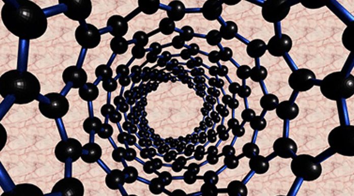
Wrocław University of Science and Technology’s Department of Polymer and Carbonaceous Materials is focused on the synthesis, characterisation and application of carbon-based nanomaterials, including nanostructured carbon materials such as carbon nanofibres and nanotubes, graphene materials, and nanoporous carbon materials.
These carbon nanomaterials and their nitrogen-doped derivatives are primarily used for electrochemical energy storage devices such as supercapacitors, lithium-ion batteries and electrochemical sensors. Nanoporous carbon materials are used as adsorbents in water treatment and gas separation including CO2 capture as well as hydrogen and methane storage.
Moreover, the research team is currently developing the graphene-based composites with conductive polymers and transition metal compounds as new-generation electrode materials for high-performance supercapacitors.
Nanoscience at Wrocław University
Several groups are involved in the research where nanostructures of various kinds (plasmonic nanoparticles, semiconductor nanostructures, carbon particles, thin sheets of minerals) are used to modify the properties of composite materials, mostly polymer-based, intended for applications ranging from construction to electronics.
The Advanced Materials Engineering and Modelling Group is focused on the optical properties of various nanostructures, especially those intended for biophotonics applications involving the use of short pulse (femtosecond or picosecond) laser excitation.
The work carried out to date has included the evaluation of nonlinear optical properties of various nanostructures (plasmonic nanoparticles such as gold nanorods and nanoshells, noble metal clusters, semiconductor quantum dots and nanoparticles of various geometries, lanthanide-doped nanocrystals, core-shell structures, etc.).
Applications of such structures for nonlinear microscopy, remote sensing of temperature and detection of biologically important analytes have also been studied.
The Department of Organic and Pharmaceutical Technology uses nanotechnology to design and fabricate nanostructure-based drug carriers. The investigated structures make use of custom-designed surfactants and other components; the cargo carried within the custom nano-containers has included photodynamic therapy sensitisers as well as other components that may help in obtaining theranostic (therapeutic and diagnostic) action.
Also, strong scientific output comes from the Faculty of Fundamental Problems of Technology, which employs 150 academic staff and hosts 1,800 students. It incorporates six departments and covers three research disciplines: physics, biomedical engineering and computer science.
Theoretical Physics
In the Department of Theoretical Physics, several groups develop their understanding of fundamental properties and phenomena in a wide class of nanosystems, nanostructures and nanomaterials, including: semiconductor quantum dots; dashes; rings and other ‘artificial atoms and molecules’; and nanoscale objects of various content and geometry, such as layers and surfaces (especially graphene and its semiconductor analogues) under extreme conditions such as ultralow temperature or high magnetic field.
The common theme of the above topics is ‘low-dimensional physics’, a vibrant area in modern physics spotlighted by the 2016 Nobel Prize. These studies have a strong computational component and benefit from the university’s own top 500 computer cluster ‘BEM’.
An important context of these studies is application in storage and the processing of quantum information and in future scalable quantum computation. The related topics include encoding, decoherence, protection of quantum information and various issues of manipulation of physical properties on the atomic scale.
Wrocław University of Science and Technology’s Department of Experimental Physics hosts the Laboratory for Optical Spectroscopy of Nanostructures (LOSN), with research focusing on physical properties of novel nanostructures, nanomaterials and new semiconducting systems, e.g. transition metal dichalcogenides, including their two-dimensional crystals or new solid-alloy multinary compounds, and related devices.
The core of activity is the application of various complementary optical spectroscopy techniques for the investigation of semiconductor-based nanostructures and nanodevices. Experimental methods are supported by theoretical modelling of the band structure and carrier kinetics.
The LOSN collaborates with technological laboratories all over the world; however, some of the materials are also fabricated at the LOSN, which includes the exfoliation of atomic layer thin crystals of the dichalcogenides or synthesis and the functionalisation of colloidal nanocrystals of various material systems.
Most of the research aims at exploring the application potential of these materials in modern optoelectronics (lasers, detectors, solar cells, gas sensors), nanophotonics (sources of single photons or entangled photon pairs, thresholdless nanolasers), or bio-medicine (biomarkers, drug carriers), also with fundamental subjects such as two-dimensional electronic gases in the regime of fractional quantum Hall effect or quantum electrodynamics in solid state systems, many body excitations and the condensation of light matter-coupled quasi-particles in semiconductor structures.
Nano-oriented research is also carried out in the Department of Quantum Technologies (nanoplasmonics, quantum cryptography, etc.) and in the Department of Biomedical Engineering (drug delivery, bioimaging, and personalised therapies).
Faculty of Microsystem Electronics and Photonics

Another centre of nanotechnological research at WUST exists at the Faculty of Microsystem Electronics and Photonics. It hosts 55 academic staff, 44 PhD students, and about 800 BSc and MSc students, incorporating seven research divisions, and holds the highest (A+) national mark of research excellence.
The Division of Microelectronics and Nanotechnology conducts research in materials science, nanotechnology, micro- and nanoelectronics, and optoelectronics. The main topics are bandgap engineering, technology of III-V heterostructures, advanced physicochemical and electrical characterisation (e.g. by electron microscopy, atomic force microscopy, X-ray diffraction, impedance spectroscopy and photoluminescence).
Epitaxial and lithographic techniques, manufacturing of metallic structures, surface passivation, spatial structuring and complex device processing are developed.
The available equipment permits full investigation cycles – from computer simulations, through technology and construction design, to implementation and characterisation of demonstrators made of advanced semiconductor devices.
The Division of Micro- and Nanostructures Metrology conducts research work aimed at the quantitative and qualitative observation of phenomena occurring on a submicron and nanometre scale. Research employs advanced microscopy close interaction, scanning electron microscopy and focused ion beam microscopy, impedance spectroscopy, X-ray diffraction, optoelectronics and fibre optics.
The Division of Technology and Diagnostics of Microelectronic Structures conducts research on fabrication of thin-films by means of physical deposition from the gas phase (in particular, magnetron sputtering and electron beam evaporation), design of functional coatings, diagnosis and analysis of electrical, optical, structural and functional properties of thin-films, analysis of electrical and optical properties of thin-film materials using numerical modelling, and studies of electrical activity of deep doping levels in low-dimensional semiconductor structures.
The Division of Microengineering and Photovoltaics at Wrocław University of Science and Technology focuses on the fabrication and characterisation of MEMS- and MOEMS-type silicon, glass and polymer microsystems, multiparametric measurement systems with integrated electronic sensors, miniature medical and biomedical devices using nano- and microengineering techniques, vacuum nano- and microelectronics, development of nano- and microengineering solid state technologies, standalone photovoltaic systems and their use in zero-energy facilities, including sports and recreational facilities and long-term studies of green energy installations.
Research in the field of nanoscience and photonics conducted at the Faculty of Electronics is mainly located in the laboratories of the Division of Laser and Fiber Electronics. Its main scientific interest is focused on ultrafast fibre and solid state lasers with saturable absorbers based on low-dimensional nanomaterials such as graphene, carbon nanotubes, topological insulators, black phosphorus and transition metal dichalcogenides.
In the well-equipped laboratories at the Faculty of Electronics pioneering research on nonlinear optical properties of nanomaterials as well as on new structures of saturable absorbers are conducted. Parallel to the fundamental research in this field, the division is working on practical applications. One example of such philosophy is the prototype of the mode-locked fibre laser using the graphene-based saturable absorber. The developed laser with amplifier is used as an effective tool for supercontinuum generation, biomedical experiments and precise laser micro-machining.


