A research team from the University of Surrey (UoS) has successfully increased the levels of energy absorbed by wafer-thin photovoltaic panels by 25%.
How do these photovoltaic solar panels work?
UoS’ photovoltaic solar panels are approximately one micrometre thick (1μm) and converts light into electricity more efficiently than others that are around the same size. Thus, this novel creation paves the way to make it easier to generate clean, green energy.
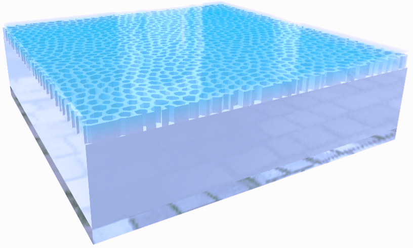
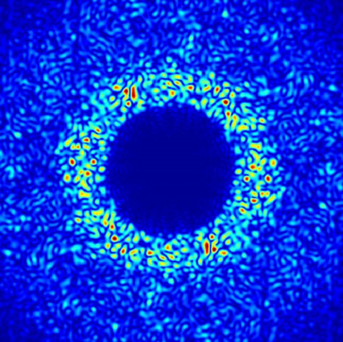
In a paper published in the American Chemical Society’s Photonics journal, the team detail how they utilised the characteristics of sunlight to design a disordered honeycomb layer, which lies on top of a wafer of silicon.
Their approach is echoed in nature, in the design of butterfly wings and bird eyes. The innovative honeycomb design enables light absorption from any angle and traps light inside the photovoltaic solar cell, enabling more energy to be generated.
Dr Marian Florescu from UoS’ Advanced Technology Institute (ATI) explained, “One of the challenges of working with silicon is that nearly a third of light bounces straight off it without being absorbed and the energy harnessed. A textured layer across the silicon helps tackle this and our disordered, yet hyperuniform, honeycomb design is particularly successful.”

How was this technology developed?
The team of researchers from UoS worked with experimental collaborators at AMOLF in Amsterdam to design, model, and create the novel ultra-thin photovoltaic solar panels.
In the laboratory, they accomplished absorption rates of approximately 26.3 mA/cm2, which is a 25% increase on the previous record of 19.72 mA/cm2 that was attained in 2017. Furthermore, they secured an efficiency of 21% but predict that further improvements will push the figure even higher, thus resulting in efficiencies that are significantly better than many commercially available photovoltaic solar panels.
As well as benefiting solar power generation, the discoveries could also benefit other industries where light management and surface engineering are crucial. This can include photo-electrochemistry, solid-state light emission, and photodetectors.
Next, the team intends to investigate commercial partners and develop manufacturing techniques, in order to make this technology readily available.
Dr Florescu concluded: “There is enormous potential for using ultra-thin photovoltaics. For example, given how light they are, they will be particularly useful in space and could make new extra-terrestrial projects viable.
“Since they use so much less silicon, we are hoping there will be cost savings here on Earth as well, plus there could be potential to bring more benefits from the Internet of Things and to create zero-energy buildings powered locally.”
To keep up to date with our content, subscribe for updates on our digital publication and newsletter.


